

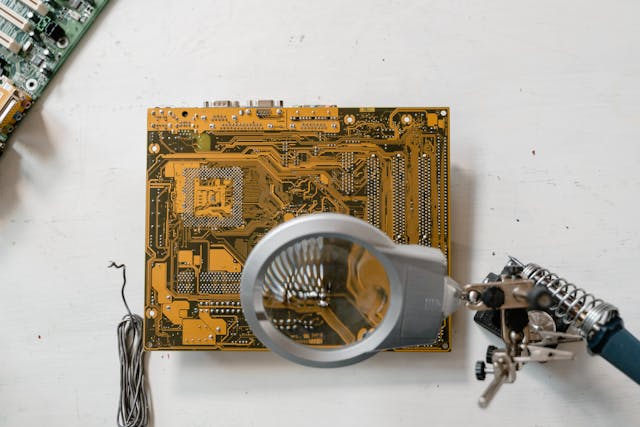
Semiconductors help to keep the modern world running. They sit inside almost all products that we use, starting from phones and laptops to cars, solar panels, and medical devices. They also help to power data centers, AI tools, and all the connected gadgets that make life easier.
But the real thing doesn’t just happen in the chip’s circuits. It starts with the thin film technologies, which are the invisible layers making those chips faster, smaller, and more reliable.
As semiconductors keep getting smaller and becoming more complex, these thin coatings play a bigger role now. They control how electricity moves, how heat spreads, and how long each chip lasts.
In this post, we’ll cover:
- What thin film technology is
- How it’s used in semiconductor manufacturing
- Why purity and precision matter
- How companies like VEM help make it all possible
What Are Thin Film Technologies?
A Simple Explanation
Thin film technology involves adding extremely thin layers of material onto a base surface, which is called the substrate. Each of those layers can be a few nanometers thick, which is thousands of times thinner than a human hair in comparison.
These layers are what make integrated circuits and many other electronic devices. In short, it makes the chips work in the way we want them to.
To create these thin films, manufacturers are using controlled methods like
- PVD (Physical Vapor Deposition): In this method, the material is vaporized in a vacuum and forms a coating.
- CVD (Chemical Vapor Deposition): In this method, a chemical reaction at high temperature creates the film.
- ALD (Atomic Layer Deposition): This builds the film one atomic layer at a time for extreme precision.
Each method serves a different purpose, which depends on what part of the chip is being built.
Why Thin Films Are Essential in Semiconductor Manufacturing
Building Smaller, Faster and More Efficient Devices
Chips become faster as well as smaller with each subsequent generation. Moore’s Law states that the number of transistors on a chip doubles about every two years. This is possible with thin films.
They allow engineers to create microscopic layers and circuits carrying electricity, isolate chip components, and shield against heat as well as corrosion.
If thin films are the arteries, semiconductors are the heart of technology.
Electrical and Functional Benefits
| Thin Film Function | Material Type | Purpose in Chips |
| Conductive Layers | Copper, Aluminum | Carry electric current |
| Barrier Layers | Titanium, Tantalum Nitride | Stop metals from mixing |
| Dielectric Films | Silicon Dioxide, Hafnium Oxide | Provide insulation |
| Reflective Layers | Gold, Silver | Improve light performance |
| Protective Coatings | Tungsten, Platinum | Prevent corrosion and wear |
These layers appear everywhere in a chip, starting from gate oxides that control switching to interconnect metals linking millions of transistors together to mirror coatings, which are used in lithography systems.
Each thin film has one goal which is to make chips perform better and last longer.
The Role of Thin Film Deposition in Semiconductor Manufacturing
Precision at the Atomic Level
Building a chip requires atomic-level accuracy. Each thin layer must be even, clean, and pure. Even a single particle of dust can cause a failure later in production.
That’s why thin film deposition happens in tightly controlled environments. Vacuum-based methods like PVD and sputtering ensure a clean, stable process.
Main Stages of Thin Film Deposition
- Target preparation: Choose the right high-purity material.
- Deposition: Apply the layer through sputtering, evaporation or ALD.
- Inspection: Check the film’s thickness, surface as well as consistency.
- Cleaning: Remove any contamination before the next layer is added.
PVD and Sputtering: The Heart of Thin Film Manufacturing
In PVD, atoms from a solid material known as target are vaporized inside a vacuum chamber and settle on the wafer surface, creating an even coating.
However, Sputtering works in a different way. Ions hit the target material, knocking loose atoms that attach themselves evenly to the wafer. This technique gives strong, uniform layers with excellent purity and adhesion.
These coatings may only be a few atoms thick, but they define how every chip performs.
Why Purity and Consistency Matter
At this level, even the smallest impurity can change how a chip behaves. That is why semiconductor manufacturers depend on partners supplying high-purity materials and perfectly bonded components.
Companies like VEM provide sputtering targets, bonding services and thin film materials that meet strict standards. Their work ensures every deposited layer stays consistent across thousands of wafers.
Real-World Impact: How Thin Films Shape the Semiconductor Industry
From Microchips to Memory Devices
Thin films define how devices perform. In microprocessors, they improve switching speed along with reducing the heat. In memory chips like DRAM and NAND flash, they make data storage faster and more reliable.
Because thin films control electrical flow and insulation, they directly affect power efficiency, performance as well as durability which are all critical in today’s devices.
Enabling Advanced Nodes and 3D Designs
Modern chips are no longer flat. Engineers are now building 3D structures using extremely thin layers handling both vertical and horizontal connections.
Technologies at 7 nm, 5 nm and 3 nm scales rely heavily on thin film precision to manage heat, resistivity and signal integrity. Without these coatings, miniaturization would hit a hard limit.
Supporting Sustainability and Recycling
Thin film processes don’t just improve performance, they also help make semiconductor manufacturing greener.
By reclaiming precious metals such as gold, platinum and palladium from used targets, manufacturers reduce waste and save resources.
VEM supports this effort through its precious-metal reclaim programs, helping the industry stay sustainable while maintaining high quality.
Challenges and the Future of Thin Film Technologies
Overcoming the Limits of Miniaturization
As chips get smaller, controlling thin film uniformity becomes harder. When a layer is only a few atoms thick, even a slight defect can cause issues.
Researchers are developing new materials such as hafnium oxide, and tantalum nitride to handle these challenges. These materials help maintain performance and stability at nanoscales.
Innovations on the Horizon
The future of thin films is moving toward more control, smarter systems, and better testing.
Here are a few trends shaping what’s next:
- Atomic Layer Deposition (ALD): builds precise nanolayers with atomic-level accuracy.
- Hybrid PVD-CVD processes: combine two methods to coat complex structures.
- AI-driven monitoring: uses data to adjust conditions instantly during production.
- Advanced purity testing: ensures zero contamination in every batch.
Each innovation aims to make semiconductor manufacturing faster, cleaner, and more efficient.
Why Reliable Partners Matter in Chip Making
Making chips takes teamwork. Factories need suppliers who deliver pure materials, steady quality, and fast help. A small delay or impurity can stop the whole line.
The Need for Trusted Thin Film Suppliers
Thin films are at the heart of modern chips. To stay on track, fabs depend on partners who can meet strict goals with speed and care.
What Makes a Great Thin Film Partner
- Proven, ISO-certified quality systems
- Strong knowledge of PVD and bonding
- Fast response and custom support
- Full help from start to reclaim and analysis
VEM offers all these. Their skill in thin films helps chip makers meet deadlines and tough standards.
Thin Films: The Hidden Power of Modern Chips
Thin films are tiny, but their role is huge. They make devices faster, smaller, and more efficient. They help batteries last longer and improve data speed.
From labs to large fabs, thin films drive new advances in chips. They are the hidden layer that keeps Moore’s Law alive—building the next wave of tech, one atom-thin sheet at a time.
FAQs
Q1. What are thin films in semiconductors?
They are very thin layers that control how chips work.
Q2. How does PVD help chip making?
PVD places even, pure layers in a vacuum, which improves chip strength and speed.
Q3. Why do we need high-purity materials?
Impurities cause defects. Pure materials keep chips steady and long-lasting.
Q4. What are today’s big challenges in thin films?
Keeping films even at the nano level, stopping defects, and finding better materials.